‘Quantum technologies in space’ – just another invention from the scientific ivory tower or already relevant to our everyday lives?
Space technologies are an integral part of our everyday lives as a result of their use in satellite communications, satellite navigation and Earth observation. Quantum technologies are based on quantum physics and will not only significantly improve space-based applications in the coming years, but also enable further innovations.
Where does DLR fit in?
DLR has been working on the development of quantum technologies for space for 20 years. The task now is to transfer the extensive development expertise for new technologies in Germany from the laboratory into applications together with companies.
Together with German companies, DLR is developing highly stable and high-precision optical clocks suitable for use in space, such as the iodine clock, which is to be tested on the Bartolomeo platform of the ISS as part of the COMPASSO project. Due to their outstanding stability, these clocks have the potential to improve the accuracy and resilience of positioning with navigation satellites and represent an excellent foundation for high-precision global timekeeping and future scientific missions.
The properties of quanta can be used to physically encrypt not only satellite communications securely, but also any form of digital communication in general. This requires a device that can perform quantum key distribution (QKD). The DLR research institutes are developing such QKD terminals suitable for use in space and on CubeSats. In the long term, these technologies will contribute to the future European quantum communication infrastructure.
Quantum sensors can also be used in Earth observation to measure Earth’s gravitational field even more precisely and thus monitor changes in the global water balance – for example ice sheets and fluctuations in sea level and groundwater. DLR is involved in the development of a pathfinder mission under the leadership of the German Space Agency at DLR together with CNES and other European partners as part of the EU project CARIOQA-PMP.
In addition, fundamental physics theories such as the theory of relativity can be tested with new quantum experiments in space and broaden our view of the Universe. To this end, the DLR institutes and the German Space Agency at DLR are working with NASA to develop the new BECCAL experimental facility for the ISS, where German and US research into ultracold atoms and Bose-Einstein condensates will be conducted jointly.
All developments in quantum technology in space are based on compact, space-qualified key components such as laser systems, frequency combs and atom chips, for which Germany is a world leader in development and microintegration. The German Space Agency at DLR supports development projects such as Leibniz University Hannover’s atom chip system for generating Bose-Einstein condensates and laser technology at the Ferdinand-Braun-Institut in Berlin with funding from the Federal Ministry for Economic Affairs and Climate Action (BMWK).
Finally, quantum computers and quantum algorithms, also in combination with artificial intelligence, offer potential for space-related applications such as complex optimisations for the autonomy of spacecraft or big data applications in Earth observation. The DLR Quantum Computing Initiative is contributing to this.
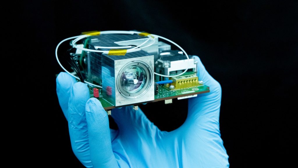
QKD terminal for cubesats
Laser terminal for the transmission of quantum states from low-Earth orbit to the ground for global quantum key distribution
The emerging second quantum revolution brings with it new innovative services based on new quantum technologies. One of the most important is quantum key distribution (QKD), an application of quantum communications. The first fibre-based products are already commercially available. However, the range of quantum communications in the fibre is limited to a few hundred kilometres. The use of satellites for transmission enables quantum key distribution on a global scale.
DLR is designing new systems and developing components for satellite-based quantum key distribution. One core component is the QKD terminal for cubesats. It enables the transmission of quantum states from Low Earth Orbit (LEO) to the ground – and does so with an extremely compact laser terminal design. It is used in two satellite missions, QUBE and QUBE2, which are at different stages of development. The special optical design supports the two wavelength ranges of around 850 and 1550 nanometres. An active mirror enables the required precise alignment of the transmission beam with the receiving station.
Links:
German Aerospace Center (DLR)
Institute of Communications and Navigation
E-Mail contact-dlr@DLR.de
COMPASSO
Quantum optical technologies for the future of satellite navigation
In the COMPASSO project, an iodine laser clock, a laser terminal and an optical frequency comb, which have been developed at DLR, will be tested under space conditions on the International Space Station ISS. These components will be installed on the Bartolomeo platform, which is mounted on the exterior of the European Columbus research module.
For use in space, optical technologies must be particularly compact, robust and durable. The development of the various components is currently under way. After they have been proven on the ISS, they will be made ready for use in the European Galileo satellite navigation system.
Compact, highly stable laser-optical clocks can significantly improve the performance of future generations of satellite navigation systems, such as Galileo. In addition, optical connections (laser links) between the satellites and to the ground infrastructure have the potential to significantly increase the accuracy of positioning on Earth. At the same time, the complexity and size of the ground infrastructure could be reduced.
COMPASSO is one of the largest projects in the Galileo Competence Center, which was founded in 2019, and will be carried out in close cooperation with industrial partners.
Link:
German Aerospace Center (DLR)
Galileo Competence Center
E-Mail contact-dlr@DLR.de
Optical iodine frequency reference
Development of an optical frequency reference for applications in space, including future Galileo, Earth observation, science
The COMPASSO mission involves research into optical clock and link technologies on the Bartolomeo platform of the International Space Station ISS. One of the central payload elements is an iodine-based optical frequency reference, which is being developed at the DLR Institute of Quantum Technologies.
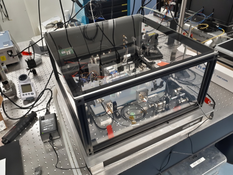
The iodine-based frequency reference has a very high frequency stability and is a possible candidate for an alternative clock technology for future generations of the European Galileo satellite navigation system. It makes use of the hyperfine splitting of the line spectrum of the iodine molecule, in which a laser is stabilised to such a resonance at a wavelength close to 532 nanometres. The iodine reference is recommended by the demonstration on the ISS – not only for the next generation of navigation satellites, but also for other applications, for example in space missions for space exploration and Earth observation.
Link:
German Aerospace Center (DLR)
Institute of Quantum Technologies
E-Mail contact-dlr@DLR.de
Atom chip system
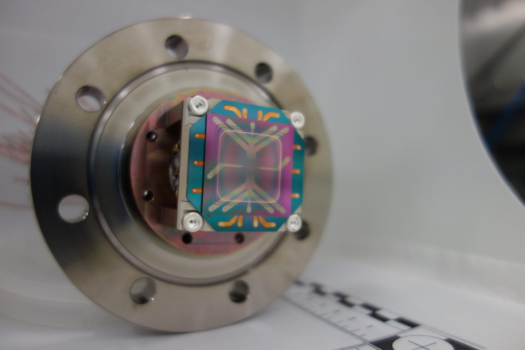
Multichip atom chip system consisting of a science and base chip and a ceramic carrier system
Atom chips are a core component of magneto-optical traps for compact matter wave interferometers. These are used in basic research to investigate the properties of Bose-Einstein Condensates (BEC) in microgravity (as in the BECCAL project), but are also intended for use as highly sensitive quantum sensors, as is being pursued in the European CARIOQA initiative for gravity field measurements, for example.
The Institute of Micro Production Technology at Leibniz University Hannover, in cooperation with the Institute of Quantum Optics, is developing atom chips as components of magneto-optical traps for compact matter wave interferometers. In combination with complex laser cooling and an external magnetic field, these atom chips with their planar conductor structures generate magnetic field configurations in order to fix atoms using the Zeeman effect and to generate BECs and use them as test masses for interferometry.
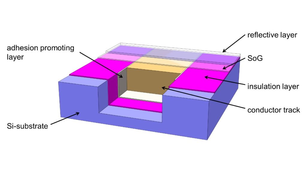
Given that operation takes place under ultra-high vacuum conditions, the use of non-adhesive bonding techniques is a top priority. Our approach relies on conductive traces embedded in the substrate. The substrate is a silicon wafer into which a 10 to 20 micrometre deep ‘trench’ has been etched, which is then electroplated with the trace material and finally planarised.
An additional bonding layer such as titanium or chrome is used to improve the adhesion of the conductor layer and prevent delamination. These chips must now be joined to a carrier system. As the operation of the atom chip is influenced by external magnetic fields, only non-magnetic materials are used throughout the atom chip system. The use of conductive materials, aside from the actual conductor tracks, is also avoided in order to suppress eddy currents. The carrier not only has the task of holding the atom chip and providing space for the electrical feedthroughs, but also contains the mesoscopic structures in the form of wires.
Links:
Institute for Micro Production Technology at the University of Hanover
https://www.impt.uni-hannover.de/en/
Micro-integrated laser technology (Ferdinand-Braun-Institut, Leibniz-Institut for High Frequency Technology)
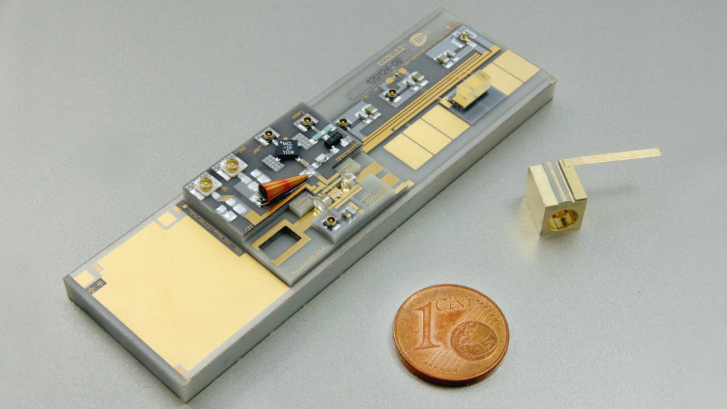
ECDL vs. mECDL – Extended cavity diode laser and monolithic-integrated device
Hybrid micro-integrated module: Extended Cavity Diode Laser (ECDL)
An edge-emitting laser diode (near the centre of the module) receives optical feedback from a ‘far’ volume holographic Bragg grating (the ‘glass block’) to stabilise its emission frequency. Lasers such as these are used for applications with the highest demands on spectral stability (for example for optical atomic clocks and atom interferometer-based acceleration sensors or for coherent free-space communication). The module was developed as part of the DLR-funded LasUS project and successfully used in the KaLExUS high-altitude research rocket mission (TEXUS 53) for potassium spectroscopy in space. A successor version was used in MAIUS-II for experiments with ultracold rubidium and potassium atoms.
mECDL
In order to further advance miniaturisation and robustness, the Ferdinand-Braun-Institut at the Leibniz-Institut für Höchstfrequenztechnik has begun developing a monolithically integrated extended cavity diode laser (mECDL) as part of the DLR-funded mECDL/ROSC project. Here, the elements of optical amplification (the laser diode in the hybrid micro-integrated approach described above), optical delay (free-space propagation of the laser beam between the laser diode and the above holographic Bragg grating) and frequency selectivity (the above holographic Bragg grating) are integrated into a single opto-electronic semiconductor component. For this purpose, an active waveguide section (for optical amplification) is combined with a low-loss, passive waveguide section (for optical delay) and a low-loss, passive Bragg waveguide section (for frequency-dependent optical feedback).
Unique characteristics
- monolithic (chip-scale design, robust, highly efficient)
- utilises a recently developed advanced two-stage epitaxy technology
- very narrow spectral linewidth
Technical specifications
- 3 dB linewidth: 25 kHz @ 1 ms (1064 nm)
- 44 mW of optical power (1064 nm) at injection current of 200 mA
MiLas®
Technology platform for space-compatible diode laser modules
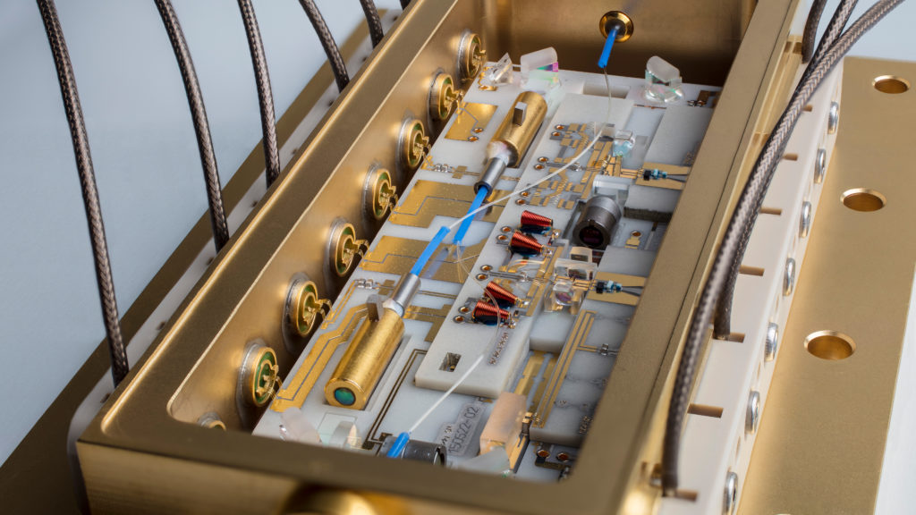
The MiLas® technology platform enables the realisation of various types of miniaturised electro-optical modules. These include, for example, master oscillator power amplifiers (MOPA), two-stage optical amplifiers or phase modulators with power amplifiers. They are used in quantum sensor technology based on cold atoms (such as atomic interferometers and optical clocks), in laser metrology (interferometry) and in coherent communication. MOPA have already been successfully used in the DLR-funded MAIUS-II and JOKARUS projects and are also planned for BECCAL and COMPASSO.
The modules consist of a micro-optical bench (MIOB) integrated into a Kovar housing. The MIOB consists of lithographically structured aluminium nitride substrates, which are assembled into a stack using precision soldering. The structuring provides functionality similar to printed circuit boards and the stacking allows a complex electrical multilayer design. All optical elements such as lenses, mirrors, optical isolators and prisms are actively aligned and bonded with a resolution and accuracy of 100 nanometres. The thermal control of critical elements is ensured by micro-Peltier elements, for example for the volume holographic Bragg grating of the master oscillator.
The electrical design includes transistors with a bandwidth of several gigahertz, which are arranged very close to the laser chips to achieve high-bandwidth current modulation.
Technical data of the ECDL-MOPA
- Output power: > 500 mW at 1064 nm from single-mode, polarisation-maintaining optical fibre
- Linewidth: 26 kHz @ 1 ms, < 1 kHz intrinsic linewidth, demonstrated with a 1064 nm ECDL MOPA
- Tunability: ~ 50 GHz (coarse), up to 50 GHz (continuous), depending on mode of operation
- High bandwidth current modulation capability (>1 GHz)
- Space-qualified technology
- Vibration load up to 8 gRMS successfully demonstrated
- Wavelengths: 767 / 780 / 871 / 1064 / 1070 nm, others on request
Miniaturised optical isolator
For the protection of diode lasers against optical feedback
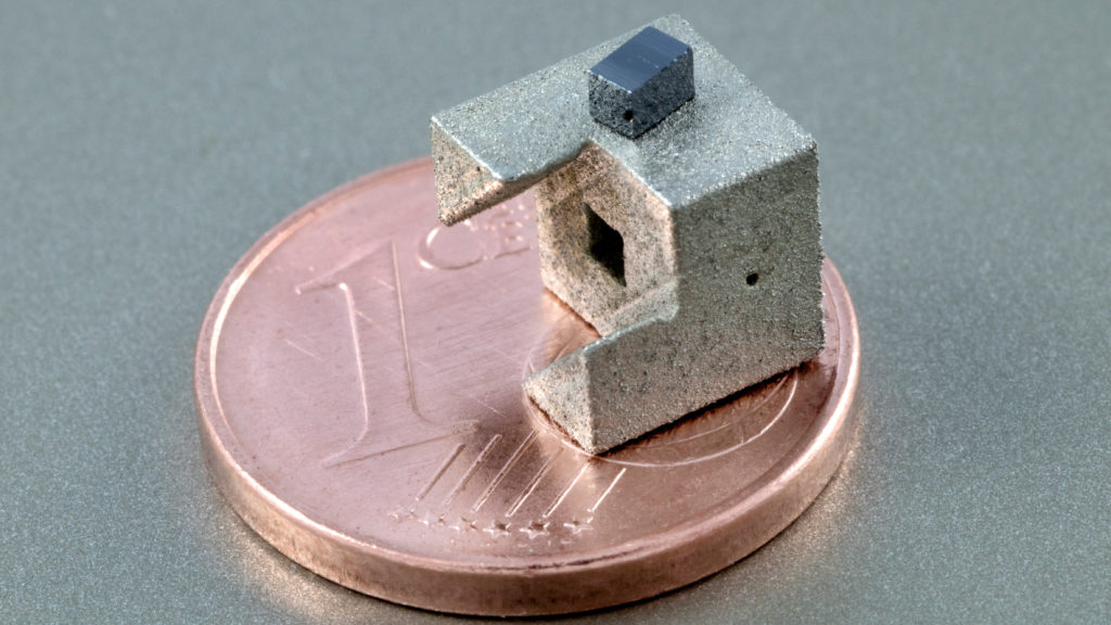
Optical isolators are elements that transmit light in a direction-dependent manner. They are used to protect diode lasers from optical feedback, which can impair electro-optical performance or even damage the component.
The miniaturised isolators are designed for applications such as quantum sensors, for example compact optical atomic clocks and quantum computers. They are being developed as part of the DLR-funded Faraday project and used for various wavelengths in the SOLIS and OPUS projects, which are also funded.
This platform can be used for the integration of isolators for wavelengths between around 400 and 950 nanometres. Due to their compactness, they are ideally suited for use in diode laser-based laser systems, which are subject to strict limitations in terms of size, mass and power consumption.
The targeted wavelength range closes a gap in the availability of commercial products and enables new applications in the field of optical quantum technologies, where ultra-compact, laser-based light sources are required.
Specifications
- Volume: 0.3 ml (6.5 mm x 6.5 mm x approx. 7 mm)
- Free mechanical aperture: 1.5 mm x 1.5 mm (suitable for a beam diameter (1/e²) of approx. 600 μm)
- different magneto-optical materials can be used to achieve an adaptation to a specific wavelength:
- Terbium-gallium-garnet (TGG) / terbium-scandium-aluminium-garnet (TSAG): for λ ~400 nm – 560 nm
- Cd1-xMnxTe for λ ~560 nm – 950 nm, with x = 0.08 … 0.50
- high remanence magnet: FeNdB alloy
- Isolation > 30 dB possible, depending on magneto-optical material
- Low insertion loss of a few 0.1 dB possible, depending on the magneto-optical material
- Example: optical isolator for 461 nm (TSAG):
- Isolation > 40 dB
- Insertion loss: 1.4 dB (27.5 %)
- Example: optical isolator for 689 nm (Cd0.50Mn0.50Te)
- Isolation > 23 dB
- Insertion loss: 1.2 dB (25%)
- Outgoing polarisation corresponds to the incoming polarisation
Links:
Ferdinand-Braun-Institut, Leibniz-Institut für Höchstfrequenztechnik
